APPLICATION NOTE 006
Benjamin Bacon, Owner, Plane Space Design
The MISO models that are designed to have the voltage source connected to their MAIN input be greater than the voltage connected to their SECOND input are not provided with a means to ensure that this condition is enforced. The external circuit can provide for the maintenance of this condition, but if that is not done the chance that SECOND will become greater than MAIN exists.
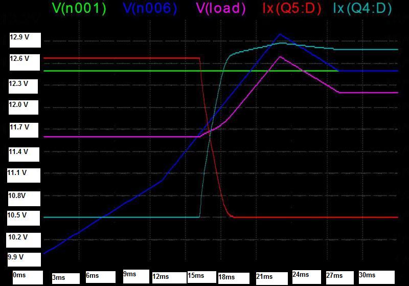
The plot shown above is the results of a PSPICE simulation that represents the case where the source connected to SECOND becomes greater than the source connected to MAIN. In the plot the curve labels and the MISO unit connection points that they represent are as follows.
| MISO UNIT ELEMENT | PLOT LABEL |
|---|---|
| MAIN | V(n001) |
| SECOND | V(n006) |
| Current from MAIN | Ix(Q5:D) |
| Current from SECOND | Ix(Q4:D) |
| MISO Output Voltage | V(load) |
The test circuit was simulated as if the Pulsed Driver was replaced by the impedance of the power resistor in the pulsed driver circuitry. The simulation proceeded as follows. The SECOND input voltage climbs from 10.0V to 13V in Piece-Wise Linear steps. The MAIN input voltage stays fixed at 12.5V. The time length of the simulation is 30 milliseconds.
The results of the simulation showed that the output current from MAIN persists on the load until the SECOND voltage rises to equal the MISO Output Voltage. At this point the SECOND current starts to increase rapidly and the MAIN current starts to decrease rapidly. As the voltage on SECOND continues to increase more current comes from this source and less current comes from MAIN. The sources pass through a current sharing point where they both provide the same magnitude of current to the load. This point is reached in less than 1 millisecond.
By the time the voltage at SECOND rises to equal the voltage at MAIN virtually all of the load current comes from SECOND. Eventually, as SECOND becomes greater than MAIN, the current from MAIN to the load stops.
Some key points to notice are:
As soon as the voltage at SECOND equals the voltage at the MISO Output, the Output voltage begins to track the voltage connected at SECOND.
The current sharing point is rapidly reached as the initial current changes are fast; and it is not long afterwards that SECOND is the primary current provider.
Also note that for the same voltage levels, SECOND supplies more current to the load than MAIN. That is because MAIN also has the task of providing current to a network of resistors that controls the switching behavior of the circuit. SECOND does not have this additional requirement and therefore puts all of its current into the load.
The channel that hosts MAIN is not off, but is only suppressed by the SECOND channel in terms of its share of the current sharing responsibilities. This means that MAIN does not have to rise to its switch-on voltage to be restored to dominance. That only needs to happen if the MAIN channel is switched off by falling below its switch-off voltage (12V in this case). In this case MAIN remains above its switch-off voltage for the entire duration so it will regain dominance if or when the voltage on SECOND falls.
The behavior that was obtained for the circuit in this simulation is reversible. That is, as the voltage at SECOND decreases along the same path, the currents and load will reverse along their same paths as well.